What are the Things to Contemplate whereas Hiring A Flexible Circuit Board Manufacturer

Nowadays printed circuit boards have become synonymous to digital units. Such board varies vastly from their design to their capabilities. And thus if you are literally hiring any company for designing and pcba manufacturing your circuit boards care must be taken about the quality and product of work they’re supplying. So for all you newbies out there starting off on this planet of digital units this is your 101 checklist to think about earlier than hiring any PCB manufacturing company. If you find yourself hiring any flexible circuit board manufacturers step one is to test their experiences. Remember regardless of how a lot begin-studded the educational career be a new company will take their time in designing your prototype. Designing actual-life prototypes are a unique style of games and thus if you are in hurry together with your flex PCB board it is always advisable that you just choose any experienced company with growing and deploying prototypes for a number of gadgets and in multiple domains. However, if you’re a lover of all that’s is experimental and on the lookout for some game-altering concepts and never agile prototyping then selecting new businesses beaming with inventive concepts may be your right choose.

The world of Flexi circuit boards are large and huge. PCB boards are a fancy field the place a variety of circuits are built-in and chipped for creating compact boards of assorted fashionable high-end circuit devices. So whereas hiring versatile circuit boards manufacturers checking their expertise is fine however make sure that their skills tallies up along with your discipline of digital units is even more vital. Remember hiring experienced companies with talents that do not tallies up along with your needs might end in heavy loss. Technology is an ever-changing domain. And all related companies ought to carry on updating themselves with the newer inclusions. PCB manufacturing business can be no totally different. So when you find yourself choosing up your manufacturing company keep in mind that they are going to be your peer for designing the prototype. So be sure that the manufacturing company you are deciding on is at par all the latest technologies and uses the identical for designing your prototype.

The flexibility to customizing the prototype design has always been an interesting quality. Sometimes regardless of how much completely you design the prototype there are some traces or loops left within the design. Also at occasions, you are feeling like improvising the design at such times make certain your manufacturing friends know how to include those add-ons. Remember the terms of services varies from company to firm. However, it’s all the time greatest to choose those who present you a comprehensive service. Sometimes after building the prototype there appear some loops within the design which must be fastened. It’s at all times best to choose those firms who cover for fixing all the faults publish prototype supply. Apart from these vital ones guantee that the agency you choose have a fame across the nation, together with software proficiency and experience over a various vary of PCB creation. So examine all the requisites stringently and select your PCB friends now.

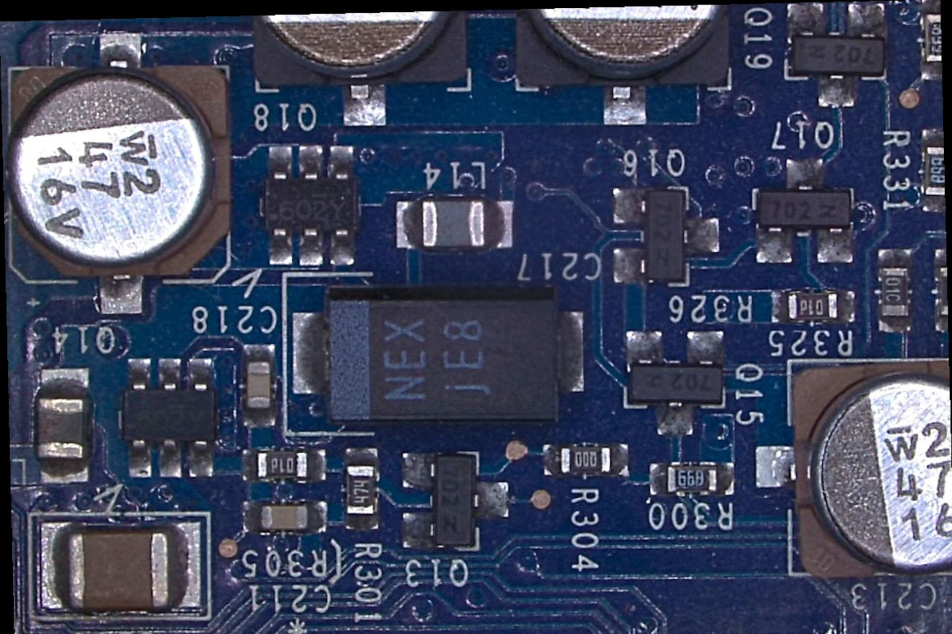
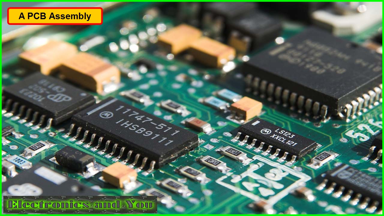
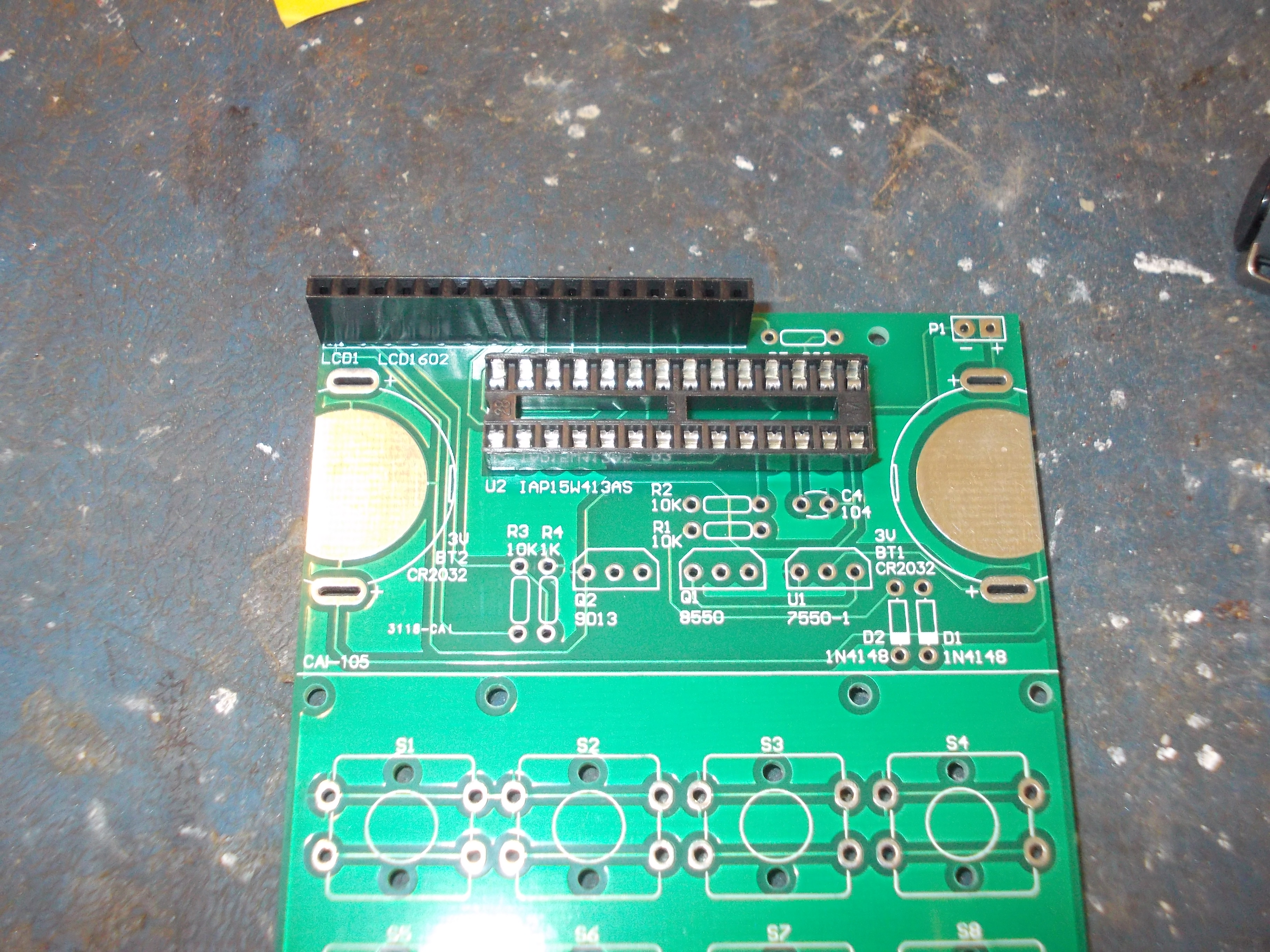
The method by which the naked printed circuit boards, PCBs utilized in electronic products is evey bit as vital as the assembling with elements. PCB manufacture fundamentals How to decide on the best PCB manufacturer The PCB manufacturing process is very important for anybody involved within the electronics trade. Printed circuit boards, PCBs, are very extensively used as the premise for digital circuits. Printed circuit boards are used to supply the mechanical basis on which the circuit could be constructed. Accordingly virtually all circuits use printed circuit boards and they are designed and utilized in portions of hundreds of thousands. Although PCBs form the idea of nearly all electronic circuits as we speak, they are typically taken without any consideration. Nevertheless technology on this space of electronics is transferring forward. Track sizes are reducing, the numbers of layers within the boards is growing to accommodate for the elevated connectivity required, PCB assembly and the design guidelines are being improved to make sure that smaller SMT devices may be handled and the soldering processes utilized in manufacturing will be accommodated.

The PCB manufacturing process may be achieved in a selection of ways and there are quite a lot of variants. Despite the various small variations, the main phases within the PCB manufacturing course of are the same. Printed circuit boards, PCBs, might be made from a wide range of substances. The most generally used in a form of glass fibre based board often known as FR4. If you liked this informative article and you desire to get more details about pcb assembly, visit the following website, generously check out the internet site. This provides an affordable diploma of stability under temperature variation and is doesn’t breakdown badly, whereas not being excessively expensive. Other cheaper supplies are available for the PCBs in low cost industrial merchandise. For prime efficiency radio frequency designs where the dielectric constant of the substrate is essential, and low ranges of loss are needed, then PTFE primarily based printed circuit boards can be used, though they are far harder to work with. In an effort to make a PCB with tracks for the components, copper clad board is first obtained. This consists of the substrate material, usually FR4, with copper cladding usually on each sides.

What are the Standards For PCB Inspection?

Sockets on PCBPrinted circuit board (PCB) inspection is a important step in ensuring quality and reliability across the electronics manufacturing course of. Both bare boards and assembled PCBs should be fastidiously examined to validate acceptability earlier than shipment to customers. But what particular criteria represent a proper PCB inspection? Read on for an overview of inspection targets, standards, metrics, tools, and key defect varieties checked during the PCB inspection course of. Thorough inspection in opposition to established standards minimizes transport defective boards to prospects. Manufacturers generally define an inspection plan with accept/reject criteria mapped to these standards. IPC standards particularly provide a framework for deciphering the severity of certain defects. Tracking metrics gives knowledge to constantly enhance processes and product high quality over time. Automated Optical Inspection (AOI) – Imaging system scans boards at high decision capturing any defects. Computer algorithms analyze images towards CAD information to detect discrepancies. Solder Mask Inspection – Validating uniformity and accuracy of solder mask utility. Checking for voids, skinny areas, misregistration.

Dimensional Inspection – Measuring important attributes like board thickness, lengths, gap positions. Confirming inside specified tolerances. Hole Wall Integrity – Testing plated by-hole conductivity and plating high quality using methods like automated flying probe electrical testing. X-Ray Imaging – Captures defects inside boards like cracks, delamination, voiding, drilling errors. Thermal Stress Testing – Subjecting boards to thermal shock, pcba guide cycling, and dwells reveals latent material stresses and workmanship points via failure analysis. Cross-Sectioning – Cutting micro-sections to examine plating thickness, resin fill, glass weave, and different inner board particulars under microscope. Bare board inspection focuses on design, fabrication, and materials high quality prior to parts being mounted. Bill of Materials (BOM) Accuracy – Confirming appropriate elements installed in every designators place. Polarity – Verifying part orientation matches footprint polarity. Presence/Absence – Detecting missing elements not mounted or incorrect quantities. Component Value – Validating correct nominal worth components put in like correct resistor resistance or capacitor values.

Placement Accuracy – Checking location placement precision against CAD centroid positions. Solder Joint Quality – Inspecting that solder fillets, toes, and bonds meet acceptability criteria. Foreign Object Debris (FOD) – Checking no free particles, dirt, debris, or hair exists on the meeting. Mechanical Assembly – Ensuring no bent leads, visible damage, board warpage, discoloration, or scorching. Electrical Tests – Running in-circuit exams (ICT), boundary scans, and functional exams to confirm proper electrical performance. Assembled board inspection focuses on components, soldering, and performance pre-shipment. Missing tremendous pitch marking. Automated Optical Inspection (AOI) – Vision cameras with sophisticated algorithms rapidly scan boards towards CAD fashions detecting discrepancies. Can examine solder joints, elements, PCB features, markings, and more. High throughput inline operation. Automated X-Ray Inspection (AXI) – X-ray imaging reveals hidden defects and confirms BOM, placement, and solder joint quality without destructive dismantling. Especially helpful for dens chips, BGAs, and QFNs. Solder Paste Inspection (SPI) – Validates quantity, space, peak uniformity, and print registration of solder paste deposits by way of 3D optical metrology.

In-Circuit Test (ICT) – Electrical probes take a look at nodes throughout circuits verifying right functionality. Fixtures enable repeatable probe alignment. Bed of Nails Test – Spring-loaded test pins make electrical contact at testpoints across board checking continuity, shorts, and opens. Flying Probe Test – Automated probe mechanism touches down at all check nodes in a programmed sequence without use of a fixture for electrical verification. Automated inspection replaces manual visible checking with fast, objective, repeatable assessment in opposition to acceptance criteria thresholds. Every product usually maintains a custom-made guidelines based mostly on important characteristics and dangers assessed from prior builds. What magnification is used to inspect PCBs? Solder joints, machined options, and positive pitch components require magnification. Handheld microscopes range from 10x to over 100x. Machine imaginative and prescient cameras present up to 200x magnification. What are common PCB inspection failure factors? Typical defects are skinny/insufficient solder, missing or incorrect parts, poor solder fillets, pads lifted from board, scorched areas, flexed boards, and debris inclusions.

Automation for PCB Assembly - Festo USA
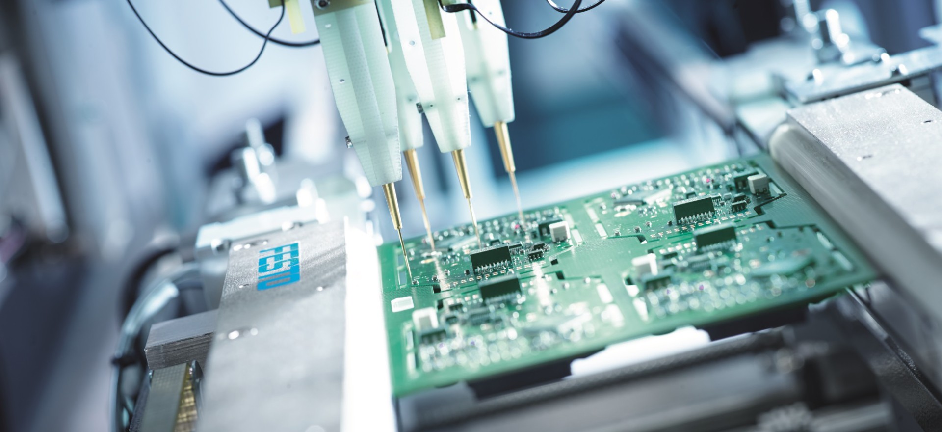
How does automated optical inspection (AOI) work? AOI compares pictures of board options to CAD data using subtle algorithms to determine discrepancies in the location, assembly, and soldering revealing any defects. Does PCB inspection impression manufacturing price? Automated inspection integrates inline without slowing general price. Manual inspection can turn into a bottleneck. AOI presents 10x the inspection factors per hour in comparison with manual. What info should PCB inspection reviews contain? Reports convey photos/details of every defect discovered, measurement knowledge, defect counts, process functionality metrics, repair suggestions, and cross/fail standing relative to acceptance standards. Rigorous PCB (urlscan.io) inspection in opposition to established acceptability criteria ensures high quality and reliability. Both naked boards and assembled PCBs endure extensive automated optical, electrical, and practical verification using metrics defined by requirements. Passing scrutiny across parameters like soldering, parts, board fabrication, and electrical operation supplies confidence previous to shipment. By institutionalizing robust inspection practices as a core self-discipline, electronics manufacturers cut back escapes, discipline failures, and ensure buyer satisfaction. It is strictly forbidden to straight take a look at the Tv, audio, video and other tools with out energy isolation transformer with the tools that’s grounded.

What are the Factors For PCB Inspection?

The Basics of A Printed Circuit Board: How Does a Circuit Board Work?
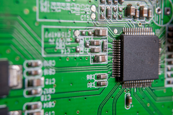
Printed circuit board (PCB) inspection is a critical step in making certain quality and reliability throughout the electronics manufacturing course of. Both naked boards and assembled PCBs must be rigorously examined to validate acceptability before shipment to customers. But what specific criteria constitute a correct PCB (www.mapleprimes.com) inspection? Read on for an overview of inspection targets, requirements, metrics, tools, and key defect sorts checked throughout the PCB inspection course of. Thorough inspection towards established criteria minimizes delivery defective boards to prospects. Manufacturers typically define an inspection plan with settle for/reject standards mapped to these standards. IPC requirements particularly provide a framework for interpreting the severity of sure defects. Tracking metrics supplies knowledge to continuously improve processes and product quality over time. Automated Optical Inspection (AOI) – Imaging system scans boards at excessive resolution capturing any defects. Computer algorithms analyze images in opposition to CAD information to detect discrepancies. Solder Mask Inspection – Validating uniformity and accuracy of solder mask application. Checking for voids, skinny areas, misregistration.

Dimensional Inspection – Measuring critical attributes like board thickness, lengths, hole positions. Confirming within specified tolerances. Hole Wall Integrity – Testing plated via-gap conductivity and plating quality utilizing methods like automated flying probe electrical testing. X-Ray Imaging – Captures defects inside boards like cracks, delamination, voiding, drilling errors. Thermal Stress Testing – Subjecting boards to thermal shock, cycling, and dwells reveals latent materials stresses and workmanship issues by failure analysis. Cross-Sectioning – Cutting micro-sections to examine plating thickness, resin fill, glass weave, and other inner board details beneath microscope. Bare board inspection focuses on design, fabrication, and material high quality previous to parts being mounted. Bill of Materials (BOM) Accuracy – Confirming correct elements put in in each designators position. Polarity – Verifying half orientation matches footprint polarity. Presence/Absence – Detecting missing parts not mounted or incorrect portions. Component Value – Validating correct nominal worth elements put in like appropriate resistor resistance or capacitor values.

Placement Accuracy – Checking location placement precision against CAD centroid positions. Solder Joint Quality – Inspecting that solder fillets, toes, and bonds meet acceptability standards. Foreign Object Debris (FOD) – Checking no free particles, dirt, debris, or hair exists on the meeting. Mechanical Assembly – Ensuring no bent leads, seen injury, board warpage, printed circuit board buy discoloration, or scorching. Electrical Tests – Running in-circuit exams (ICT), boundary scans, and practical exams to affirm correct electrical performance. Assembled board inspection focuses on components, soldering, and performance pre-shipment. Missing positive pitch marking. Automated Optical Inspection (AOI) – Vision cameras with subtle algorithms quickly scan boards against CAD fashions detecting discrepancies. Can examine solder joints, elements, PCB features, markings, and extra. High throughput inline operation. Automated X-Ray Inspection (AXI) – X-ray imaging reveals hidden defects and confirms BOM, placement, and solder joint high quality with out destructive dismantling. Especially useful for dens chips, BGAs, and QFNs. Solder Paste Inspection (SPI) – Validates volume, space, peak uniformity, and print registration of solder paste deposits by way of 3D optical metrology.

In-Circuit Test (ICT) – Electrical probes take a look at nodes throughout circuits verifying right functionality. Fixtures enable repeatable probe alignment. Bed of Nails Test – Spring-loaded test pins make electrical contact at testpoints across board checking continuity, shorts, and opens. Flying Probe Test – Automated probe mechanism touches down in any respect test nodes in a programmed sequence without use of a fixture for electrical verification. Automated inspection replaces handbook visible checking with fast, goal, repeatable assessment in opposition to acceptance criteria thresholds. Every product usually maintains a personalized guidelines primarily based on crucial traits and PCB dangers assessed from prior builds. What magnification is used to inspect PCBs? Solder joints, machined features, and fine pitch parts require magnification. Handheld microscopes range from 10x to over 100x. Machine imaginative and prescient cameras provide as much as 200x magnification. What are common PCB inspection failure factors? Typical defects are thin/insufficient solder, missing or incorrect elements, poor solder fillets, pads lifted from board, scorched areas, flexed boards, and debris inclusions.

Ergodox Kebyboard Pcb Design 3d animation branding computer design electronics graphic design illustration logo motion graphics pcb design ui vectorHow does automated optical inspection (AOI) work? AOI compares pictures of board features to CAD data using subtle algorithms to determine discrepancies in the location, assembly, and soldering revealing any defects. Does PCB inspection impact manufacturing fee? Automated inspection integrates inline without slowing overall rate. Manual inspection can turn out to be a bottleneck. AOI affords 10x the inspection points per hour compared to guide. What information ought to PCB inspection studies include? Reports convey images/details of each defect discovered, measurement data, defect counts, process functionality metrics, restore recommendations, and move/fail standing relative to acceptance criteria. Rigorous PCB inspection towards established acceptability criteria ensures quality and reliability. Both naked boards and assembled PCBs undergo extensive automated optical, electrical, and useful verification using metrics outlined by requirements. Passing scrutiny throughout parameters like soldering, components, board fabrication, and PCB electrical operation provides confidence previous to shipment. By institutionalizing robust inspection practices as a core self-discipline, electronics manufacturers reduce escapes, area failures, and ensure customer satisfaction. It is strictly forbidden to straight take a look at the Tv, audio, video and different tools with out energy isolation transformer with the tools that’s grounded.

Small Batch PCB Assembly for Prototypes And Low Volume

Small batch PCB assembly or low quantity PCB assembly refers to 5 to 30 items of printed circuit boards to be soldered with electronic elements. The PCB assembly producer PCBONLINE provides one-cease solutions for low-volume PCBA, no matter how advanced the circuit is, together with embody DFM, DFT, DFX, PCB fabrication, part sourcing, seeking different components, PCB board PCB assembly, and end-product meeting. In case your Gerber, BOM, and decide-and-place file are all okay and PCB board we have now all components in stock, our low-quantity PCB manufacturing and assembly can begin instantly, and the turnaround time is 24 hours. If we do not have all elements in stock, we want additional 12 hours or more to source all the opposite elements. So in such a case, the minimal turnaround time for low-volume PCB assembly is 36 hours. On the 24-hour PCB manufacturer PCBONLINE, small-batch PCB manufacturing and meeting are carried out on the same production strains as bulky PCB manufacturing and assembly. This ensures quality conformity.

Low-volume PCB assembly is low-cost PCB assembly, although the price of low volume PCB assembly is set by varied elements, together with together with the place the manufacturer is positioned, PCB measurement, varieties of PCB, testing, complexity, and digital parts. We will not set the PCB assembly price vary merely in response to the board quantity, but often, low-quantity PCB assembly is cheaper than excessive quantity. In case you are shopping for an OEM PCB assembly service and getting the field constructed, the average value of the low-quantity PCB assembly is lower than for those who solely order the PCB assembly. As for the value issue – location, Shenzhen of China is the place you will get good high quality PCB at a low worth. In U.S. and Europe, where suppliers also provide high quality PCB and assembly, PCB board the price is very high, and the turnaround can be much longer. While in different regions the PCB know-how just isn’t that developed and chances are you’ll spend even more as a result of the standard is not ensured and in that case, you will buy again from different suppliers. So if you’d like quality and low-cost PCB assembly, choose small-run PCB manufacturers in China. PCBONLINE is your greatest selection for low-price PCB assembly. The low-quantity PCB manufacturer PCBONLINE has absolute advantages in expedited small-batch PCB assembly orders. Flexible manufacturing: PCBONLINE gives flexible production. Now we have capabilities and wealthy experiences to meet the totally different wants of different clients for low-quantity PCB assembly.

The method by which the bare printed circuit boards, PCBs utilized in digital merchandise is evey bit as essential because the assembling with elements. PCB manufacture fundamentals How to decide on the proper PCB manufacturer The PCB manufacturing course of is essential for anybody concerned within the electronics trade. Printed circuit boards, PCBs, are very extensively used as the premise for electronic circuits. Printed circuit boards are used to supply the mechanical foundation on which the circuit can be built. Accordingly just about all circuits use printed circuit boards and they’re designed and used in quantities of hundreds of thousands. Although PCBs type the basis of nearly all electronic circuits right now, they are usually taken for granted. Nevertheless technology on this space of electronics is shifting ahead. Track sizes are reducing, the numbers of layers in the boards is rising to accommodate for the increased connectivity required, and the design guidelines are being improved to ensure that smaller SMT gadgets could be handled and the soldering processes used in manufacturing will be accommodated.

The PCB manufacturing process can be achieved in a selection of ways and there are various variants. Despite the various small variations, the primary phases in the PCB manufacturing course of are the identical. Printed circuit boards, PCBs, might be made from quite a lot of substances. The most generally used in a form of glass fibre primarily based board often called FR4. This provides an inexpensive diploma of stability below temperature variation and is doesn’t breakdown badly, while not being excessively costly. Other cheaper supplies can be found for the PCBs in low price industrial merchandise. If you loved this information and you would certainly such as to obtain more info relating to PCB board (click through the following post) kindly visit the website. For high performance radio frequency designs the place the dielectric constant of the substrate is necessary, and low ranges of loss are needed, then PTFE based printed circuit boards can be used, although they’re far harder to work with. In order to make a PCB with tracks for the parts, copper clad board is first obtained. This consists of the substrate material, typically FR4, with copper cladding normally on each sides.

Rigid-Flex PCB Board Design Guidelines

File:910CX-2 PCB side view.jpg - Wikimedia CommonsThere are important selections and concerns to make for a profitable inflexible-flex PCB design course of at an early stage. These are important if you happen to want to keep up its reliability and reduce prices. Are you a inflexible-flex PCB designer searching for some design principles? This text is for you. What is Rigid-Flex PCB? Rigid-Flex PCB is a board that combines inflexible board applied sciences and flexible circuits. The manufacturing course of tends to be much like a conventional hardboard circuit, however some layers are versatile circuitry working throughout the hardboard. Many rigid-flex boards have a number of flexible circuit substrates layers connected to either a number of rigid boards. This can also be internally or externally relying n the kind of design utilized in the appliance. The flexible circuit substrates are designed to keep up a relentless state formed into flexed curves throughout installation or manufacturing. Rigid-flex PCB designs are extra challenging than the everyday inflexible board surroundings because the boards are made in a 3D space with greater spatial effectivity.

Project 366 #330: 251112 Board On BoardsSince it is potential to design in three dimensions, it is simple for designers to twist, fold or roll the versatile substrates to achieve the specified last form. The trendy technology is properly improved in relation to the production of giant-scale portions PCB assembly and PCB fabrication or production of a inflexible-flex prototype. The flex PCB process is sweet in overcoming weight and house issues. Careful consideration of rigid-flex solutions and correct evaluation of the various choices available is thought to have significant benefits. The PCB (https://Myspace.com) fabricator is used early through the design course of to ensure that the design and fabrication parts are in coordination and account for PCB (notes.io) ultimate product variations. The Rigid-flex PCB manufacturing process is complicated and time-consuming compared to inflexible board fabrication. Rigid-flex meeting versatile parts have different dealing with, soldering processes, and etching than the rigid FR4 Boards. Maximizing area often increases the probabilities of lower depend in parts.

With fewer solder joints, excessive connection reliability is assured. There’s a decreased weight as soon as cables and connectors between the inflexible board components and the general system get eliminated. It’s a more simplified PCB assembly course of. The dealing with course of throughout meeting is straightforward, not like with flexible boards. The test circumstances are also simplified, and a whole test before installation is feasible. Integrated ZIF contacts help in simple modular interfaces to the system’s surroundings. With Rigid-flex PCB boards, there is a big discount in logistics and assembly costs. The complexity of mechanical designs can be elevated, thus bettering the degree of freedom for optimizing housing solutions. It is important to differentiate between a rigid-flex PCB board and a flex board with stiffeners. Though stiffeners can be used for each functions, stiffeners supply some stability for assembly and mechanical functions. But, a flexible circuit with stiffeners tends to restrict where parts get placed, affecting overall component density.

Because of that, stiffeners turn out to be a consideration issue between a inflexible-flex board and flex boards with stiffeners. This is important to assist decide whether or not or not the versatile circuit wi9th stiffener gives the wanted component density desired. As element density will increase, versatile boards with stiffeners attain their limit thus, making inflexible-flex PCB extra desirable. Also, a rigid-flex board has a easy meeting course of and offers the next density for circuit routing and parts. However, if it’s not wanted, flex boards with stiffeners will probably be ample and be inexpensive. The price of a rigid-flex PCB is comparatively high in comparison with hardboards. Usually, the prices are twice or triple the worth of flexible boards with stiffeners. So, why the cost distinction? High-density functions: Rigid-flex PCB boards fold into small profiles, pcb assembly due to this fact, offering space-saving choices n each occasion. As an example, it may accommodate connectors and cables needed by electronic PCB designs. Highly dependable: Rigid-flex PCB boards provide great reliability when parts are subjected to shock and extreme vibrations.

Check these 7 Points for Selecting A PCB Manufacturer

With quite a few PCB manufacturers round, deciding on one may be difficult. Manufacturers of printed circuit board (PCB) need to have the correct of experience and expertise, and if you are inserting an order, it’s essential to examine among the necessary details. In this post, we’ve got compiled a listing of ideas that will come handy in finding the proper producer. 1. Check the fundamentals. How long has the corporate been in enterprise? It’s essential know a producer inside out and the way they do enterprise in the trade. On the subject of electronics, expertise is an side you can’t afford to take with no consideration. 2. Can they handle your necessities? That is one in all the primary questions you want to ask whenever you look for a PCB producer. Some corporations just deal with a standard set of specifications and tolerances, mainly as a result of their production capabilities are limited. If you’re in search of something very particular, you need a workforce who can handle that.

3. Who are their clients? PCB manufacturers work with various assorted purchasers within the electronics trade, and a few of them additionally deal with army orders. If you wish to know an organization better, that you must examine their clientele and the type of work they have done for others. With a reputed name, you don’t have to worry about this side, as a result of most details shall be listed on their webpage, and the rising corporations will not thoughts sharing the references on request. 4. Will they provide engineering support? That’s one of the early questions, as nicely. Before the actual cash is spent on the fabrication process, you need a company that can check all of the elements and will fully surrender to the needs of the shopper. They should take a look at the designs, so as to keep away from all doable errors sooner or later. A superb firm may also spend considerably on enhancing their prospects and capabilities. 5. Quality matters. This can be a cliche thing to say, but when it comes to PCBs, quality matters greater than anything else.

You do not to spend your assets on a company who wouldn’t guarantee that beforehand. Check their working capabilities and PCB the kind of projects they will manage for your business. With regards to high quality, you also need to know their testing course of, especially for connectivity. 6. When can they ship? Now, if you’re looking to put a fast order, you’ll want to examine this facet, as nicely. Many PCB manufacturers require greater than a few weeks earlier than they’ll deliver your order, and that’s not one thing you would expect in the primary place. 7. Can they offer certifications? Some corporations supply “UL 94V-0 fireplace resistance certification” on PCBs, and it’s possible you’ll wish to test for different relevant certifications, as nicely. In short, the worth you pay ought to be worth the products you get. Finally, do ask particulars of their vendors for materials provide. With PCBs, it’s a must to be further cautious about each aspect. Take your time to judge these features, and you may all the time thank us later.

PCB board is the mom of electronic merchandise. Most digital tools and products should be outfitted PWB Board. Printed circuit board are sometimes called PWB, even have many peoples known as PCB substrate. For the reason that printed circuit board (sqworl.com) will not be a normal terminal product, the definition of the title is barely complicated. For instance, the motherboard for personal computers is named the mainboard, and can’t be instantly referred to as the circuit board. Although there are circuit boards within the motherboard, They are not the identical, so when evaluating the trade, the two are related but can’t be stated to be the same. Another instance: as a result of there are integrated circuit elements mounted on the circuit board, the information media name it an IC board, but in truth, it is not equivalent to a printed circuit board. We usually say that the printed circuit board refers back to the naked board-that’s, the circuit board with out higher elements.

In line with the number of electronic board layers, it can be divided into single-sided, double-layer, 4-layer, six-layer, and different multilayer circuit boards. And proceed to develop in the path of high precision, excessive density, and pcba high reliability. Continuously shrinking volume, decreasing costs, and improving performance have enabled printed circuit boards to keep up strong vitality in the event of future electronic merchandise. The longer term growth development of PWB manufacturing know-how is to develop in the route of high density, high precision, effective aperture, advantageous wire, small pitch, excessive reliability, multilayer, excessive-velocity transmission, lightweight, and thinness in performance. The single layer is on an insulating substrate with a thickness of 0.2-5mm, just one floor is coated with copper foil, and a printed circuit is formed on the substrate by printing and etching. The only panel is simple to manufacture and simple to assemble. The double sided boards are printed circuits on each sides of an insulating substrate with a thickness of 0.2-5mm. It’s suitable for digital products with general necessities, comparable to digital computer systems, digital devices and meters.