The Essentials Of PCB Prototyping

A PCB (printed circuit board) prototype is a model or sample of what the ultimate PCB will look and operate like. PCB prototyping is an essential process that comes prior to mass production and the following launch of recent PCBs into the market. This process ascertains whether or not a steered PCB design will carry out as expected thereby revealing any doable flaws and thus enabling the designers to make any needed changes. Another enhancements or alternatives the designers may think of are additionally launched at this stage. The mass production of any new product leave alone PCBs can’t simply simply start without the prototyping stage. Prototyping is not going to essentially reveal any flaws as at times the design is ideal. PCB prototyping in this case shall be used confirm and re-ascertain that the PCBs performance is constant. The manufacturer or the purchasers can then give their opinion in regards to the PCB along with different solutions/improvements they may have.

Pcb Assembly - 86PCBThe PCB designers should at all times be prepared for any possible outcomes and thus any reworking at this stage ought to further not be thought of as an additional cost. Bypassing prototyping and fascinating within the mass manufacturing of a PCB just for it to fail it will definitely be catastrophic when it comes to wasted effort, time and money. The following are the generalized levels in PCB prototyping. The first known as the breadboard take a look at or proof of precept. This checks if the logic behind the PCB is achievable. If you liked this write-up and you would like to get more data regarding Pcb Assembly Review kindly stop by our own web site. Next is analyzing the size (preferable dimensions) aspects of the anticipated PCB. After this stage a visible mannequin is generated and if approved the ultimate stage which is perform and appearance is began. Whatever is achieved at this juncture is the closest to what the precise PCB will appear to be. Typically, pcb assembly review in prototyping for PCBs, the simulation of current stream within the board and the condition of the circuitry are the two most essential processes. It is just until the simulated system works as required that actual components and materials are carried out for the ultimate model or prototype. The production of prototypes is a course of limited by time – it ought to take the least time possible to pave means for the precise manufacture. Companies providing PCB prototyping companies are also more likely to be concerned in manufacture. As such, these corporations try to develop good/excellent prototypes. Advancement in know-how and more so computerization has expedited the processes of prototyping and manufacturing PCBs and made them as error-free as possible. Accordingly, pcba (tupalo.com) It’s smart to decide on a PCB firm which has the newest technology, a functionality which will make sure that the error margin is almost zero, using dangerous chemicals is avoided, and PCB sizes are stored as small as doable but just as they are as required for modern digital gadgets.

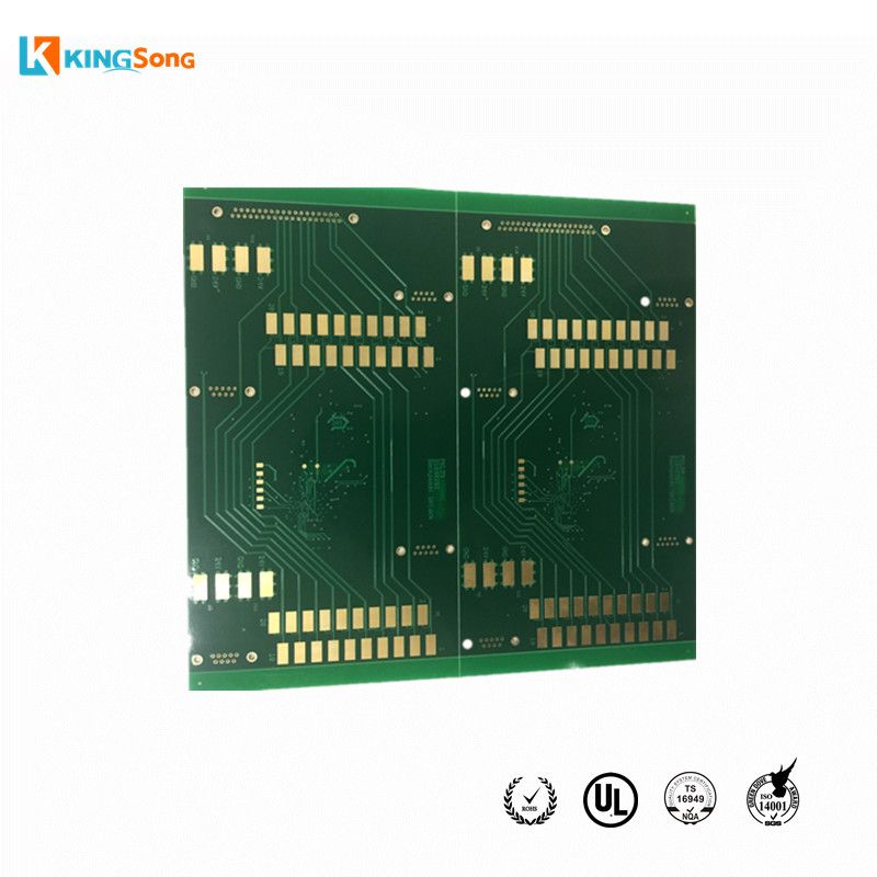
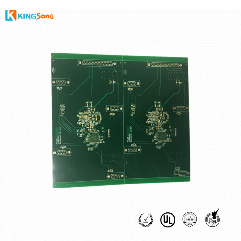
The process by which the bare printed circuit boards, PCBs used in digital merchandise is evey bit as important because the assembling with components. PCB manufacture fundamentals How to decide on the best PCB manufacturer The PCB manufacturing process is very important for anyone concerned in the electronics trade. Printed circuit boards, PCBs, are very extensively used as the idea for electronic circuits. Printed circuit boards are used to provide the mechanical foundation on which the circuit could be built. Accordingly virtually all circuits use printed circuit boards and they are designed and utilized in quantities of hundreds of thousands. Although PCBs type the premise of virtually all digital circuits today, they tend to be taken for granted. Nevertheless expertise in this space of electronics is moving forward. Track sizes are reducing, the numbers of layers within the boards is rising to accommodate for the increased connectivity required, and the design rules are being improved to ensure that smaller SMT gadgets could be handled and the soldering processes utilized in production might be accommodated.

The PCB manufacturing course of might be achieved in a variety of the way and there are a lot of variants. Despite the various small variations, the primary phases in the PCB manufacturing course of are the identical. Printed circuit boards, PCBs, may be made from quite a lot of substances. The most widely used in a form of glass fibre based board known as FR4. This offers a reasonable diploma of stability under temperature variation and is doesn’t breakdown badly, whereas not being excessively expensive. Other cheaper supplies are available for the PCBs in low value industrial products. For prime performance radio frequency designs the place the dielectric fixed of the substrate is necessary, and low ranges of loss are needed, then PTFE primarily based printed circuit boards can be utilized, though they’re far more difficult to work with. To be able to make a PCB with tracks for the elements, copper clad board is first obtained. This consists of the substrate material, typically FR4, with copper cladding normally on both sides.

The Functions and Varieties Of PCB Plates

Different materials and elements contribute to the profitable operation of a circuit board. A printed circuit board is the center of most digital devices. However, some materials are used for designing this circuit board. A PCB plate is an example of such supplies. A plate is a crucial component in a circuit board. PCBs supply each mechanical and electrical support to electronic devices. A plate is often utilized in a keyboard PCB. In this text, we’ll discuss the whole lot you have to know about PCB plates. What’s a PCB Plate? What is a PCB Plate? A PCB plate is a metal plate connected over the PCB used in a keyboard. This plate affords additional support. Also, the keys on a keyboard are straight mounted on the PCB plate and never the PCB. In addition, the PCB plate on the keyboard prevents it from bending. This plate allows the keyboard to be extra stable and strengthened.

PCB plates are usually used with greater keyboards. This is because it presents more assist. Also, the keyboard might flex more attributable to the additional dimension. However, some keyboards don’t have a PCB plate. Modern keyboards feature a plate. You possibly can select to design your keyboard with out utilizing a plate. However, the soldering high quality will determine the stability of the switches. The PCB is the constructing block of a keyboard. A keyboard features based mostly on the PCB. Everything built on a keyboard begins from the PCB. Just like the way in which a motherboard serves as the muse of a pc, so is the PCB to a keyboard. The PCB plate supplies further help when positioned on the top of the PCB. This plate helps to offer enough stability to the keyboard. Also, it prevents the keyboard from any flex. There are a number of materials used for designing a PCB. However, the 2 commonest materials used for plates are brass and aluminum. The type of fabric you use for your plate relies upon in your alternative.

However, it is sweet to explore these supplies and see what works for you. A brass plate is a really inflexible one. Also, brass is a good material for a PCB plate. However, this material can tarnish or oxidize over time if left untreated. In line with some customers, brass could be loud and bassy. This plate is very durable. Also, it’s lightweight and permits flex when typing. Therefore, carbon fiber plates offer a bouncy really feel. This material is the commonest PCB plate materials. Aluminum plates are sometimes used on prebuilt keyboards and custom. Also, aluminum is an out there material. This materials affords sturdiness and it is straightforward to chop. It’s a inflexible material that features no flex in a keyboard. This can be a plastic material. A polycarbonate plate permits flex and may be bouncy when used. However, customers maintained that this plate features a bassy sound. Plates are majorly used in keyboards.

These plates supply further assist when installed on high of the PCB used for keyboards. Plate-mounted switches: These switches require plates. Also, they feature 3-pins on the bottom. There’s a middle circular knob and two metal pins. However, they don’t have stabilization pins. That is the place the plate turns into purposeful. Therefore, this plate stabilizes each swap and minimizes facet-to-aspect wobbling anytime you press the key. Both plate mount and PCB mount characteristic the circuit board. However, the foremost distinction is if the keyboard makes use of or doesn’t use a steel plate for help. With this type of keyboard, the important thing switches can be straight mounted to the PCB. Also, a PCB mounted keyboard doesn’t require a mounting plate. This model of mounting is good for smaller keyboards. However, it isn’t preferrred for bigger keyboards. It is because the end result will be a flimsy keyboard. Using a plate mount model on a smaller keyboard may not be price it.

However, a plate mount is right for a larger keyboard. Also, it is cheaper to design a PCB mounted keyboard since it affords more flexibility. In the event you loved this article and you would love to receive details regarding PCBA (mouse click the following internet site) i implore you to visit our page. PCB mounted keyboards are very straightforward to modify. Also, they’re less expensive. Here, the important thing switches are all installed on a plate. The metallic plate is commonly put in above the PCB. Also, the designer mounts the key switches on the plate after which solders it on the PCB. A plate-mounted keyboard often takes extra time to design. Also, this mounting fashion is time-consuming and requires extra price. The plate mount type is appropriate for larger keyboards. Also, it may very well be an incredible option for a smaller keyboard. However, the end result might be a excessive-high quality keyboard. The mounting plate may be very troublesome to move. Therefore, customizations or modifications can be very troublesome to do. So, it’s advisable to desolder all key switches and resolder once achieved.

Do you Require a PCB Prototype whereas Creating The Printed Circuit Boards

The designer integrates all of the performance that may match into the board. Sometimes the necessities are in depth and the board may be each large and very complex. Many things are obligatory for the design to take it to the prototype stage. Dependability and functionality are given prime priority. The variety of layers crucial depends on the intricacy of the necessities. Some low value PCB boards are only two layers, but in detailed applications they may attain over 32 layers. Size can be essential. The board ought to match into the system it is being designed for. The tolerances utilized in most PCB design are to the thousands of an inch, making every layer and copper hint crucial. They are designed below very high tolerances and this integrity should be checked and pcba re-checked for precision. Signals ought to be clean and voltage ought to watch the applying. Components added to the floor should also fulfill the tight tolerances.

The primary board that’s created is referred to as the prototype. This will likely range in quality from one to lots of depending on the extent of the testing done. The low price circuit board undergoes excessive scrutiny. Everything ought to be checked through the manufacturing procedure. All of the leads and traces are re-measured to make sure the density earlier than the board is pressed. The holes are drilled utilizing very superior gear that has to be preprogrammed for every board. When the components are added to the floor, once more the electrical signals are tested and tolerances are checked. Once manufacturing has created the board in accordance with the specifications, the prototype is then examined and retested. Every necessity of the board must be scrutinized for efficiencies and dependability. The board is examined independently to make sure functionality before being integrated into the setting it’s designed for. Every step is documented and recorded. Any failures should be addressed fully and PCB in some cases a recent prototype with modifications must be built. This prototype remains beneath proper scrutiny until it’s performing according to expectations. Contemporary Printed Circuit Board expertise has led to a substantial discount in respect to conductor crossovers on varied planes, leading to a reduction in space requirements and enhanced packaging density in electric parts. Nonetheless, the contemporary VLSI and different multi-pin configuration units have tremendously enhanced the packaging density and consequently the focus of interconnecting strains. This has given rise to the intricate design points like capacitance, cross-speak, noise and unacceptable voltage drops as a result of parallel sign lines. These issues could not be correctly resolved in single-sided or double-sided boards, requiring an extension to the fabrication of the multi-layer circuit board.

pcb assemblyread this blog post from www.metooo.io, board is the mother of digital products. Most digital equipment and products should be equipped PWB Board. Printed circuit board are often referred to as PWB, even have many peoples called PCB substrate. For the reason that printed circuit board is not a basic terminal product, the definition of the identify is slightly complicated. For example, the motherboard for private computer systems is named the mainboard, and can’t be directly known as the circuit board. Although there are circuit boards in the motherboard, They aren’t the same, so when evaluating the industry, the two are related but can’t be stated to be the same. Another instance: because there are integrated circuit parts mounted on the circuit board, the information media name it an IC board, however in reality, it isn’t equivalent to a printed circuit board. We often say that the printed circuit board refers to the bare board-that is, the circuit board with out upper elements.

In response to the number of digital board layers, it can be divided into single-sided, double-layer, four-layer, six-layer, and different multilayer circuit boards. And proceed to develop in the path of excessive precision, excessive density, and high reliability. Continuously shrinking quantity, reducing costs, and enhancing performance have enabled printed circuit boards to keep up sturdy vitality in the development of future digital merchandise. The future development pattern of PWB manufacturing expertise is to develop within the route of excessive density, excessive precision, superb aperture, fantastic wire, small pitch, high reliability, multilayer, excessive-velocity transmission, lightweight, and thinness in performance. The one layer is on an insulating substrate with a thickness of 0.2-5mm, just one floor is covered with copper foil, and a printed circuit is formed on the substrate by printing and etching. The single panel is simple to manufacture and straightforward to assemble. The double sided boards are printed circuits on each sides of an insulating substrate with a thickness of 0.2-5mm. It is suitable for electronic merchandise with general necessities, such as digital computers, digital instruments and meters.

Since the wiring density of the double-sided printed circuit is higher than that of the one-sided printed circuit, the amount of the gadget can be diminished. Printed panel with more than three layers of printed circuits printed on an insulating substrate are referred to as multilayer panel. It’s a mix of several thin single or double panels, and its thickness is usually 1.2-2.5mm. So as to guide out the circuit sandwiched between the insulating substrate, the holes for mounting parts on the multilayer board must be metalized, that is, a metallic layer is applied to the inside floor of the small holes to connect them with the printed circuit sandwiched between the insulating substrates. The inflexible PWB has a sure mechanical strength, and the elements assembled with it have a flat state. Rigid printed panel are used basically digital merchandise. The flexible PWB is made from smooth layered plastic or other tender insulating supplies as the bottom materials. The elements product of it can be bent and stretched and can be bent according to the installation necessities throughout use.

Top 5 Rules For Manufacturing Effective PCB Design

If you want that the components of a PCB Design to work as desired, it is advisable to follow certain rules. To ensure your indicators have a reliable path to journey it’s a must to route the ability, floor and signal traces. This will also help to keep your board functioning correctly. Listed below are 5 effective set of rules to bear in mind while establishing an effective PCB Design. One of the elemental guidelines for pcb manufacturing service is to keep the facility and floor planes internally within the board. There might be an interference of excessive voltage in power circuits with low-voltage and current management circuits. Therefore, the components should even be centered and symmetrical to prevent bowing and twisting of the board. This bowing could cause elements to maneuver out of place and doubtlessly destruct the board. You can strive conserving your grounds for each power supply stage separated.

Say your floor plane is in the center layer of your board then embody a small impedance path to prevent energy circuit interference. Tracking includes connecting sign traces in line with the schematic design of the pcb manufacturing service. Be sure your traces are short and direct. Another factor, if your horizontal hint routing is on one side of the PCB, then the vertical traces must be on the other facet. The board requires multiple nets with totally different currents. This determines the width of the web additionally. You should utilize a hint width calculator to help you with this step. The dedication of the pad and hole dimensions ought to be performed early in the design process. Getting the appropriate pad-to-gap size ratio turns into harder and important as the scale of the pads and holes decreases concurrently. Situations get worse when working by way of holes. Guidelines are supplied by the producer on the requirements and facet ratio they require. The shape of the PCB pads is another essential consideration. The footprints used can differ in keeping with the manufacturing process. Larger footprints are required for wave soldering whereas infrared reflow soldering will not be obligatory. Eliminate antennas these radiate electromagnetic energy when you’re designing a PCB. Large loops of sign and ground-return lines that carry high frequencies needs to be averted. Carefully place built-in circuits to realize quick interconnect lines. A detailed ground grid is a necessary trait of RF PCB format design guideline. It helps to ensure that return strains are near the signal strains. In a multilayer board, this keeps the effective antenna space relatively small. Therefore, you possibly can obtain this with a floor aircraft. It’s best to repeatedly test your work all through the design course of. Checking is also required when the manufacturing process is going on. Should you catch problems early, it would help reduce their impact and reduce the costs of fixing them.

PCB board is the mother of electronic merchandise. Most electronic tools and merchandise need to be geared up PWB Board. Printed circuit board are also known as PWB, even have many peoples referred to as PCB substrate. Since the printed circuit board just isn’t a basic terminal product, the definition of the name is barely complicated. For instance, the motherboard for personal computer systems known as the mainboard, and cannot be straight referred to as the circuit board. Although there are circuit boards in the motherboard, They don’t seem to be the identical, so when evaluating the industry, the 2 are associated however cannot be stated to be the identical. Another instance: because there are integrated circuit parts mounted on the circuit board, the news media name it an IC board, however in fact, it is not equivalent to a printed circuit board. We often say that the printed circuit board refers back to the naked board-that’s, the circuit board with out upper components.

According to the variety of digital board layers, it may be divided into single-sided, double-layer, four-layer, pcba six-layer, and different multilayer circuit boards. And proceed to develop within the direction of high precision, high density, and excessive reliability. Continuously shrinking quantity, decreasing costs, and bettering performance have enabled printed circuit boards to maintain strong vitality in the development of future electronic products. The longer term improvement trend of PWB manufacturing technology is to develop in the path of high density, high precision, high quality aperture, effective wire, small pitch, excessive reliability, multilayer, excessive-velocity transmission, lightweight, and thinness in efficiency. The one layer is on an insulating substrate with a thickness of 0.2-5mm, just one surface is lined with copper foil, and a printed circuit is formed on the substrate by printing and etching. The single panel is easy to manufacture and straightforward to assemble. The double sided boards are printed circuits on each sides of an insulating substrate with a thickness of 0.2-5mm. It is appropriate for electronic products with general requirements, equivalent to electronic computers, electronic devices and meters.

Because the wiring density of the double-sided printed circuit is greater than that of the one-sided printed circuit, the volume of the machine can be reduced. Printed panel with greater than three layers of printed circuits printed on an insulating substrate are called multilayer panel. It is a mixture of a number of skinny single or double panels, and its thickness is generally 1.2-2.5mm. In order to lead out the circuit sandwiched between the insulating substrate, the holes for mounting elements on the multilayer board should be metalized, that is, a metal layer is utilized to the inner floor of the small holes to attach them with the printed circuit sandwiched between the insulating substrates. The rigid PWB has a certain mechanical energy, and the parts assembled with it have a flat state. Rigid printed panel are used in general electronic merchandise. Here is more info about PCBA – blogfreely.net, look into the site. The flexible PWB is made from delicate layered plastic or other comfortable insulating materials as the bottom materials. The components fabricated from it can be bent and stretched and will be bent according to the set up necessities throughout use.

Top 5 Benefits of PCB Assembly under One Roof

In relation to electronics manufacturing, some firms choose to companion with a number of companies: one for prototypes, one for manufacturing, one for testing, and so on. While this may occasionally offer upfront value savings, it could value more in the long term when you encounter delays in any links of the chain. That’s the reason many corporations opt for a single-firm PCB assembly resolution like Telan Corporation. In terms of electronics manufacturing, some firms select to companion with a number of companies: one for prototypes, one for manufacturing, one for testing, and so on. While this may supply upfront cost financial savings, it can cost more in the long term for those who encounter delays in any links of the chain. That is why many companies opt for a single-firm PCB assembly solution like Telan Corporation. One level of contact – When several corporations are concerned within the PCB process, it is way harder to keep everybody on the identical web page throughout the course of the venture.

Your product could end up handed to a unique stage of production before the earlier company realizes alterations should be made, and now you may have delays as the merchandise is shipped again for modifications. Also, if the accomplished product fails, it becomes more durable to pin down whom to contact for support. Solving these problems prices time and money, pushing back delivery to your customers. With a single-firm PCB service, any downside will be corrected with just one name to a single firm. You don’t have to worry about miscommunication as info gets handed between multiple corporations, and you can shortly get your product back on monitor. Control Every Step of the way – With just one level of contact, you also have extra management over the production process. You’ll be able to easily collaborate together with your PCB assembly service over each facet of the design. With less fingers concerned in the project, it is less complicated to ensure your wants and wants are being met on each degree.

Fast turnaround – For those who need a fast turnaround, your greatest selection is a single-company PCB assembly service in New York. You remove the delays of knowledge relays in addition to transport time between firms. With everything underneath one roof, Telan Corporation delivers prototypes in 7-10 days and normal manufacturing in 3-4 weeks. More management over prices – A multi-company PCB course of means you can be receiving a number of bills for a similar venture. And PCB since every company is looking to make a revenue, your organization now carries the burden of their income. By opting for a single-firm PCB resolution in New York, you’ll only obtain one bill and one revenue margin, allowing you to complete a mission for a fraction of the cost. Quality assurance and value-added engineering. As a part of our New York PCB assembly services, we run automated optical inspections on every product. We also consider your product to search out methods you can cut back costs and/or improve its operate. We’re proud to be in our fourth decade of providing high-high quality PCB assembly and contract electronics providers in New York. From surface mount know-how to mixed know-how, we have the capabilities you’re looking for. Contact us at the moment and put our expertise to be just right for you.

The process by which the bare printed circuit boards, PCBs used in digital products is evey bit as vital as the assembling with components. PCB manufacture basics How to choose the suitable PCB producer The PCB manufacturing process is very important for anyone involved within the electronics industry. Printed circuit boards, PCBs, are very broadly used as the premise for electronic circuits. Printed circuit boards are used to offer the mechanical foundation on which the circuit may be constructed. Accordingly virtually all circuits use printed circuit boards and they’re designed and used in quantities of hundreds of thousands. Although PCBs kind the idea of just about all electronic circuits at present, they tend to be taken with no consideration. Nevertheless expertise on this area of electronics is shifting ahead. Track sizes are decreasing, the numbers of layers within the boards is rising to accommodate for the increased connectivity required, and the design guidelines are being improved to ensure that smaller SMT units will be handled and the soldering processes utilized in manufacturing will be accommodated.

The PCB manufacturing course of can be achieved in a selection of ways and there are plenty of variants. Despite the many small variations, the main stages in the PCB manufacturing process are the identical. Printed circuit boards, PCBs, may be made from quite a lot of substances. The most widely used in a type of glass fibre based mostly board referred to as FR4. This offers a reasonable diploma of stability under temperature variation and is doesn’t breakdown badly, whereas not being excessively expensive. Other cheaper materials can be found for the PCBs in low value industrial products. For prime performance radio frequency designs the place the dielectric constant of the substrate is necessary, and low levels of loss are wanted, then PTFE based printed circuit boards can be used, although they’re far harder to work with. As a way to make a PCB with tracks for the parts, copper clad board is first obtained. This consists of the substrate materials, usually FR4, with copper cladding normally on both sides.

Small Batch PCB Assembly for Prototypes And Low Volume

Small batch PCB assembly or low quantity PCB assembly refers to 5 to 30 items of printed circuit boards to be soldered with digital components. The PCB assembly manufacturer PCBONLINE provides one-cease options for low-volume PCBA, no matter how complex the circuit is, including include DFM, DFT, DFX, PCB fabrication, component sourcing, seeking alternative elements, PCB assembly, and end-product assembly. If your Gerber, BOM, and decide-and-place file are all okay and we have all parts in inventory, our low-quantity PCB manufacturing and meeting can begin instantly, and the turnaround time is 24 hours. If we don’t have all components in inventory, we’d like extra 12 hours or extra to source all the other components. So in such a case, the minimum turnaround time for low-quantity PCB assembly is 36 hours. At the 24-hour PCB producer PCBONLINE, small-batch PCB manufacturing and assembly are carried out on the identical manufacturing strains as bulky PCB manufacturing and assembly. This ensures high quality conformity.

Low-volume PCB assembly is low-cost PCB assembly, although the price of low quantity PCB assembly is decided by numerous components, including together with where the manufacturer is positioned, PCB measurement, forms of PCB, testing, complexity, and digital elements. We won’t set the PCB assembly price vary merely according to the board amount, but normally, low-volume PCB assembly is cheaper than excessive volume. If you are buying an OEM PCB assembly service and getting the field built, the common price of the low-volume PCB assembly is lower than in the event you solely order the PCB assembly. As for the value factor – location, Shenzhen of China is where you can get good high quality PCB at a low value. In U.S. and Europe, where suppliers also present quality PCB and meeting, the worth is very excessive, and the turnaround can be for much longer. If you loved this post and you would like to get more facts with regards to printed circuit board cost kindly stop by our web site. While in different areas the PCB expertise just isn’t that developed and you might spend much more because the quality just isn’t ensured and in that case, you’ll buy once more from different suppliers. So in order for you quality and low cost PCB assembly, select small-run PCB manufacturers in China. PCBONLINE is your best choice for low-price PCB assembly. The low-quantity PCB manufacturer PCBONLINE has absolute advantages in expedited small-batch PCB assembly orders. Flexible production: PCBONLINE gives versatile production. We’ve got capabilities and rich experiences to fulfill the different needs of different prospects for low-quantity PCB assembly.

The process by which the bare printed circuit boards, PCBs used in electronic products is evey bit as necessary because the assembling with components. PCB manufacture fundamentals How to decide on the right PCB producer The PCB manufacturing process is very important for anybody involved in the electronics business. Printed circuit boards, PCBs, are very broadly used as the premise for electronic circuits. Printed circuit boards are used to provide the mechanical foundation on which the circuit will be constructed. Accordingly nearly all circuits use printed circuit boards and they are designed and used in portions of thousands and thousands. Although PCBs type the premise of virtually all digital circuits immediately, they are usually taken without any consideration. Nevertheless technology on this space of electronics is moving ahead. Track sizes are reducing, the numbers of layers in the boards is growing to accommodate for the increased connectivity required, and the design rules are being improved to ensure that smaller SMT devices can be dealt with and printed circuit board cost the soldering processes utilized in manufacturing might be accommodated.

The PCB manufacturing course of may be achieved in a variety of how and there are numerous variants. Despite the many small variations, the main levels within the PCB manufacturing process are the same. Printed circuit boards, PCBs, could be made from a variety of substances. The most widely used in a type of glass fibre based mostly board referred to as FR4. This provides an inexpensive degree of stability underneath temperature variation and is doesn’t breakdown badly, whereas not being excessively costly. Other cheaper materials can be found for the PCBs in low value commercial merchandise. For top efficiency radio frequency designs where the dielectric constant of the substrate is important, and low ranges of loss are needed, then PTFE based printed circuit boards can be used, although they are far more difficult to work with. With the intention to make a PCB with tracks for the components, copper clad board is first obtained. This consists of the substrate material, sometimes FR4, with copper cladding usually on each sides.